
Light sources are crucial in visual systems. Appropriate illumination can distinguish the target information of the object being measured from the background, resulting in high-quality, high-contrast images. This reduces the complexity of image processing algorithms while improving system accuracy and reliability. Light sources are categorized as visible, infrared, and ultraviolet light at different wavelengths. Infrared light, due to its unique advantages, is particularly prominent in the semiconductor field, where near-infrared light has a strong penetrating power. This makes it increasingly important in machine vision inspection for semiconductors.
Overview
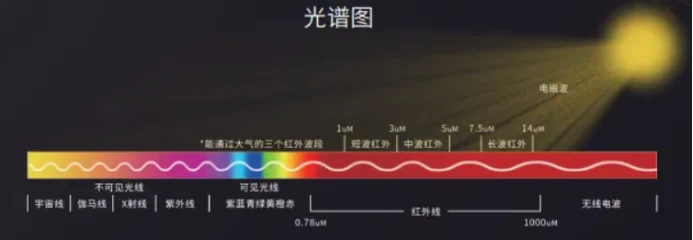
Shortwave infrared (SWIR) ranges between 900 and 2500 nm. Shorter SWIR wavelengths, from approximately 900 nm to 1700 nm, behave similarly to photons in the visible range. While the spectral content of targets in the SWIR is different, the resulting image is still sharper, unlike the lower-resolution thermal imaging of the MWIR and LWIR bands. This advantage aligns SWIR more closely with the needs of many industrial machine vision applications . Occupying the electromagnetic spectrum above the near-infrared, it is completely beyond the capabilities of traditional silicon-based imaging sensors.
advantage
So why use shortwave infrared? Because shortwave infrared has the following advantages:
● High sensitivity
● High resolution
● Able to observe under night sky glow
● Day and night imaging
● Concealed lighting
● No need for low temperature refrigeration
● Conventional low-cost visible light lenses can be used
● Small size
● Low power
application
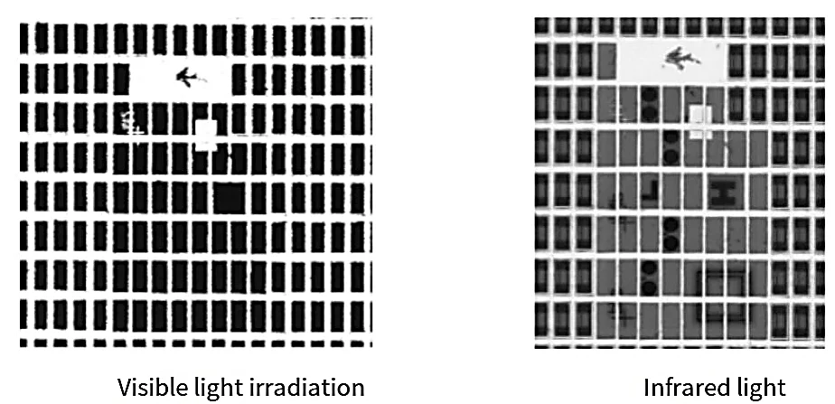
Near-infrared (NIR) is generally defined as light in the 700-2000nm wavelength range. For infrared cameras, the upper limit for silicon-based sensors is approximately 1100nm, while that for indium gallium arsenide ( InGaAs ) sensors is around 1800nm. These sensors are currently the primary sensors used in NIR microscopy, covering the typical NIR band. NIR imaging can be used to address a wide range of applications that are difficult or impossible using visible light. Certain materials, such as water vapor, silicon, some chemical compounds, and some blue films, are transparent to NIR imaging. This provides unique advantages for raw material inspection applications, such as imaging defects on and within silicon wafers. Consequently, IR microscopy is being applied across various aspects of the semiconductor industry.
In addition, infrared light is also widely used in other fields. For example, in the food industry, different materials have different absorption characteristics, which will show different colors in the image, such as distinguishing seasonings, salt, sugar, etc.; detecting whether there is damage inside the apple, distinguishing water and oil; distinguishing different plastic substances, etc.
Infrared devices
The most commonly used infrared light sources are LEDs and halogen lamps.
The advantages of LED light sources are low heat generation, low power consumption, and a longer lifespan than halogen lamps. Therefore, LEDs are the preferred light source for FA applications, which are generally used for long periods of time.
However, LED light sources lack the light intensity compared to halogen lamps, and it is difficult for a single LED light source to detect a wide wavelength range. Increasing the light intensity naturally increases costs.
Halogen lamps have the disadvantages of short lifespan and high heat generation. However, compared to LED light sources, halogen lamps offer higher light intensity and a wider wavelength. Therefore, halogen lamps are generally suitable for a wide range of wavelength analysis and testing.
The matching camera lens is generally an infrared camera and lens. The infrared camera lens responds better to infrared light, has better transmittance to infrared light, and has better imaging effect.
Conclusion
Infrared light and its imaging have unique advantages that make them suitable for a wide range of applications and industries. In particular, its ability to penetrate semiconductor materials makes it play an important role in semiconductor defect detection. However, not all materials respond to infrared bands. Therefore, knowing in advance the type of material being inspected and which wavelength it responds to is one of the prerequisites for using infrared detection.
https://www.y-crystaled.net/application-of-infrared-light-in-machine-vision-inspection.html